I've been working on getting Linux to be fully functional on an AllWinner A13 tablet. If you haven't heard, AllWinner A10 and A13 CPUs are the greatest thing since sliced bread when it comes to working with cheap hardware. A13 tablets go for $39 wholesale in China, and about $65 shipped to your door in the USA.
The open source driver for the A13 camera doesn't seem to work, so I will be trying to find out what the problem is and fix it. The plan is to tap the I2C bus that controls the camera and spy on it with a logic analyzer to see what is going wrong with the driver. This post will just cover figuring out which lines to tap into, and a follow up post will show the actual analysis of the I2C bus. This is a technique I have used successfully to fix the driver for the Goodix GT811 touchscreen.
 Generic A13 Tablet
The camera is that little round cutout at the bottom of the tablet shown above. A closeup of the camera can be seen below.
 Closeup of the Camera
Amazingly, this camera is held in place by a piece of sticky tape. Yes, sticky tape. Chinese manufacturing at its finest. But it seems to stay in place, so who am I to criticize?
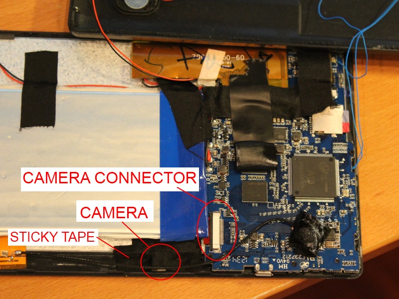
First step is to crack open the tablet. These tablets are snap together, so no screws hold the two halves of the tablet together. Below is a picture of the tablet after it has been opened up. The LCD screen is facing down against the table top, and the PCB and battery are mounted to the back of the LCD. The back of the plastic cover can be seen in the top of the picture. I have a lot of debug wires (the blue wires running everywhere) which are attached to the back plastic cover. Not all the sticky tape is from the factory, some is mine because the factory tape loses its grip after repeated removals.
 A13 Tablet Guts
Unrelated anecdote (your reading my blog so you have to listen to my ramblings too), many years ago when I was shopping for electronics in shadier parts of Hong Kong, every hawker selling questionable electronics would always claim that even though the brand was something that nobody had ever heard of, they all had "Sony guts"
In the picture above, you can see how the camera at the bottom is just held in place with sticky tape. I didn't remove all the tape holding the camera in place because I was worried it would never go back in place again. You can also see the camera connector that I am interested in.
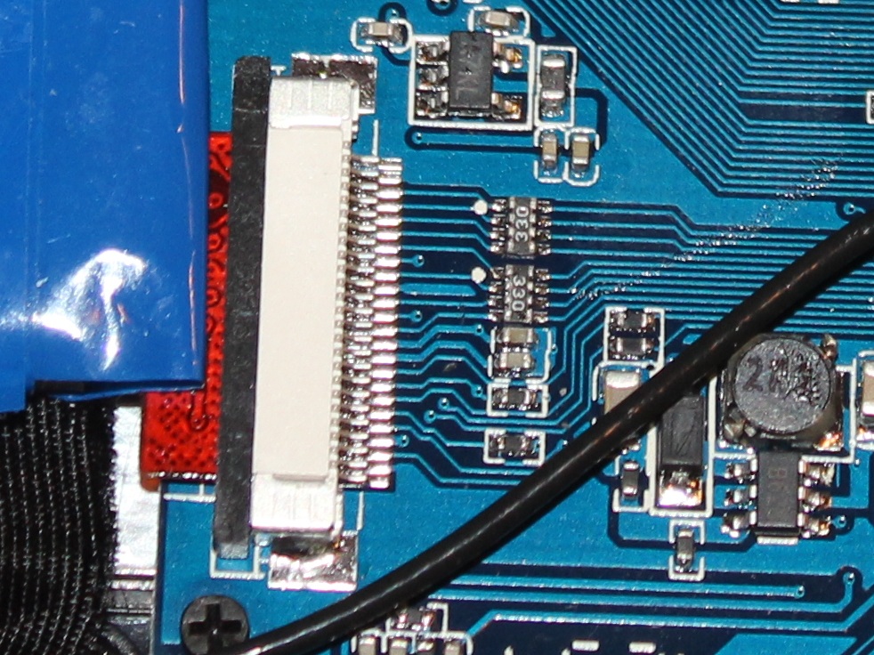
Below is a closeup of the camera connector
 Close up of the Camera Connector
So from the A13 datasheet, we know the CSI has the following signal lines:
CSI_PCLK - Pixel Clock
CSI_MCLK - Sensor Clock
CSI_HSYNC - Horizontal Sync
CSI_VSYNC - Vertical Sync
CSI_D7:0 - 8 Data lines
We also know that the tablet uses a GalaxyCore GC0308 Camera. From the GC0308 datasheet we see that it uses the following signal lines
AVDD25 - 0.1uF Filtering cap to ground
VREF - 0.1uF Filtering cap to ground
SBDA - I2C Data Line
SBCL - I2C Clock Line
D7:0 - 8 Data Lines
GND - Ground
PWDN - Powerdown signal (active high)
HSYNC - HSYNC output
VSYNC - VSYNC output
DVDD28 - 2.8V input
RESETB - Reset (active low)
INCLK - Input Clock
The 8 data lines are easy to spot with the 4 element resistor arrays protecting the data bus.
The 2 filtering caps for AVDD25 and VREF are also easy to spot.
That just leaves the 2 mystery resistors. It is easy to tell if they are the pullups required for the I2C bus by checking if the side of the resistor not connected to the flex connector are tied together and tied to 3.3V. Then we know for sure they are the pullups for the I2C data and clock lines and we can tap into the I2C signals by soldering some very fine wires to the side of the resistor that is connected to the flex connector.
After checking the voltage at the two resistors, it is confirmed that they are both at 2.8V which means they are indeed the I2C pullup resistors. (I said 3.3V, close enough)
In Part 2, I will solder fine wires to the resistors and we hook the logic analyzer up! Always fun soldering wires to 0402 resistors (Thats 0.04" x 0.02", or about the width of 2 human hairs side by side)